Difference between revisions of "Special Meeting Grounding Scheme Summary 9/22/21"
Jump to navigation
Jump to search
(Created page with "PARTICIPANTS: Carlos, Fernando, Thi, Emmanuel, Vladimir, Tanja, Brad DISCUSSION GROUND BETWEEN PCB AND ALUMINUM PART * Option to connect PCB+aluminum part * Enclosure alrea...") |
|||
| Line 11: | Line 11: | ||
* Can put provision on PCB board for additional grounding - activating this feature would take some labor though (unplug, activate, reinstall, etc.) | * Can put provision on PCB board for additional grounding - activating this feature would take some labor though (unplug, activate, reinstall, etc.) | ||
| − | * Review overview sketch of grounding (Fernando) | + | * Review [https://wiki.jlab.org/cuawiki/images/7/76/NPS-special-meeting-grounding-15Oct2021.png overview sketch of NPS grounding] (Fernando) |
::* general agreement that it captures all features of NPS grounding | ::* general agreement that it captures all features of NPS grounding | ||
::* next: put sketch into CAD for more detailed discussion | ::* next: put sketch into CAD for more detailed discussion | ||
Latest revision as of 18:42, 18 October 2021
PARTICIPANTS: Carlos, Fernando, Thi, Emmanuel, Vladimir, Tanja, Brad
DISCUSSION GROUND BETWEEN PCB AND ALUMINUM PART
- Option to connect PCB+aluminum part
- Enclosure already grounded through mechanical attachment to structure - cannot isolate detector from support structure
- mu metal shield already connected to mechanical structure
- make sure that shielding ground (through mechanical structure) is separate from electronics ground
- Can put provision on PCB board for additional grounding - activating this feature would take some labor though (unplug, activate, reinstall, etc.)
- Review overview sketch of NPS grounding (Fernando)
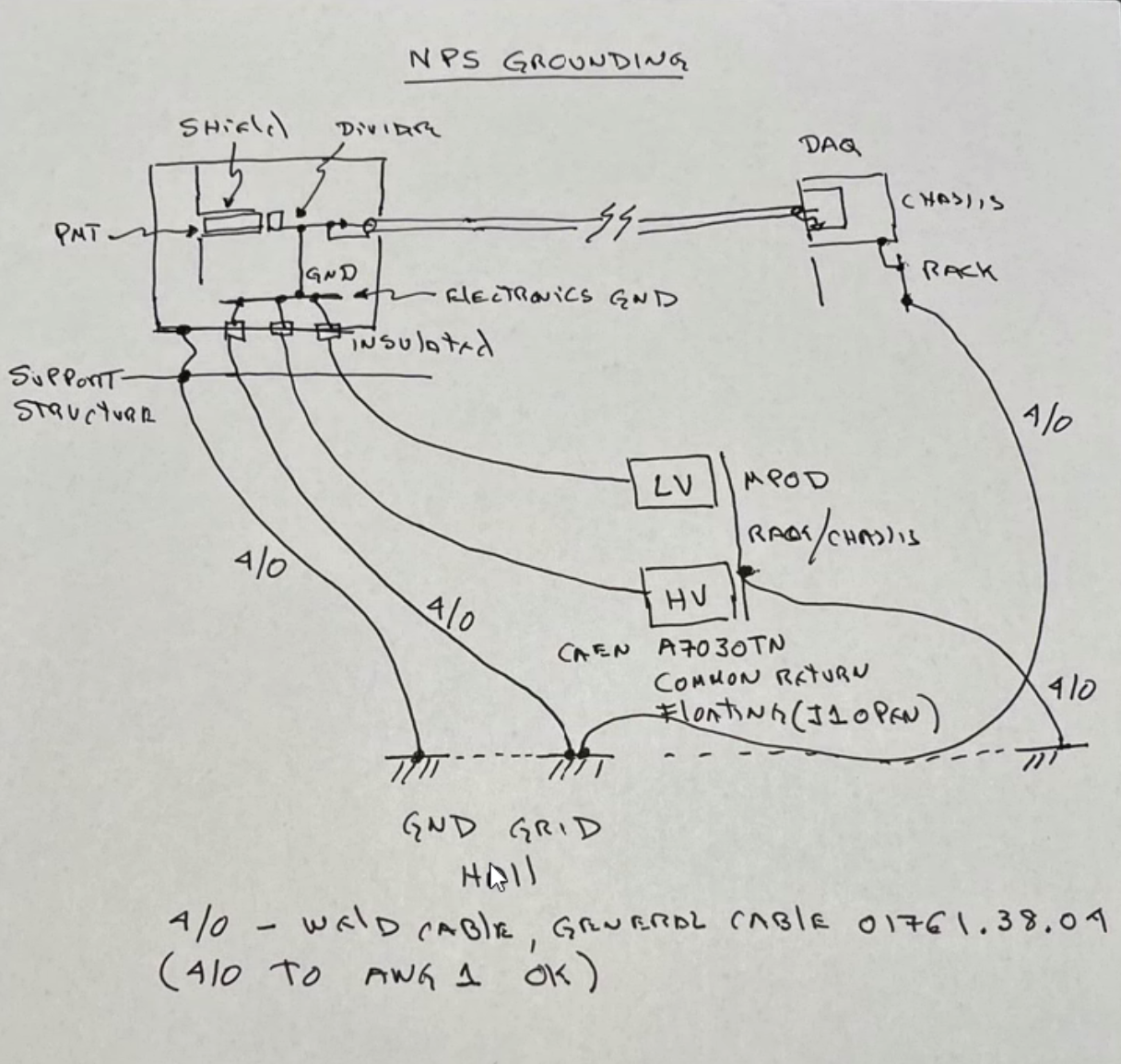
- general agreement that it captures all features of NPS grounding
- next: put sketch into CAD for more detailed discussion
- Main NPS box isolated from carriage
- How to test grounding scheme
- can do some tests in the lab - some simulations possible
- ultimately will have to test when all is assembled
- Need information on position of connector on PCB
- Action items:
- generate CAD for NPS grounding
- finalize design of PCB - need position of connector
- test optimized divider (Vladimir)
- Estimated timeline:
- finalize PCB design
- prototype new PCB and testing
- production - should be in place by end of the year