Difference between revisions of "Cables"
Jump to navigation
Jump to search
| Line 20: | Line 20: | ||
[[File:GoWTJr.png|400px]] | [[File:GoWTJr.png|400px]] | ||
| − | * The HV is distributed from the top of the board through 3 ribbon cables. | + | * The HV is distributed from the top of the board through [https://wiki.jlab.org/cuawiki/index.php?title=Cables&action=submit#HV_ribbon_cables 3 ribbon cables]. |
* The LED sitting in front of each PMT are controlled by a ribbon cable connecting at the bottom of the board | * The LED sitting in front of each PMT are controlled by a ribbon cable connecting at the bottom of the board | ||
* Anode signal from each channel get out of the board through the opposite side and through SMA connectors | * Anode signal from each channel get out of the board through the opposite side and through SMA connectors | ||
| − | * Board schematics | + | * Board schematics: [https://wiki.jlab.org/cuawiki/images/7/77/Sch%C3%A9ma_Carte_Interface.pdf 1], [https://wiki.jlab.org/cuawiki/images/2/28/Carte_Interface-1.pdf 2] |
| − | |||
== HV ribbon cables == | == HV ribbon cables == | ||
| + | [[File: HV.jpg|600px]] | ||
== LED control cables == | == LED control cables == | ||
| Line 32: | Line 32: | ||
== Patch panels at the top of the NPS box == | == Patch panels at the top of the NPS box == | ||
| + | There are 3 panels of the top of the NPS box: | ||
| + | |||
| + | [[File:NPS_frame_connector_layout.jpg|800px]] | ||
=== Signal panel (LEMO) === | === Signal panel (LEMO) === | ||
=== HV panel === | === HV panel === | ||
=== LED panel === | === LED panel === | ||
Revision as of 04:58, 25 August 2020
Voltage divider
- Voltage divider schematics
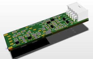
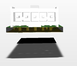
- The connector on the voltage divider is Samtec Part # IPL1-105-01-L-S-RA-K:
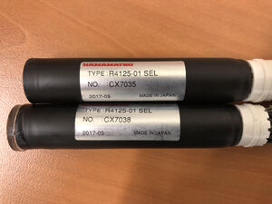
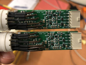
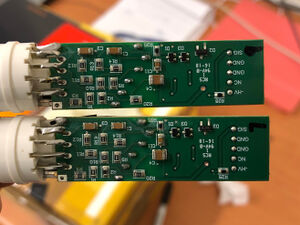
- Pictures of the assembly:
Custom cable from voltage divider to PCB boards
The cable has a SAMTEC connector IPD1-05-S-K on one side. On the other side the cable has a SMA RS PRO 546-3210 connector (Datasheet, Crimp instructions) and Fischer connector S 102 A 018. The cable length is 375 mm.
- Cable schematics
- Picture of the cable:
PCB boards (one per detector column)
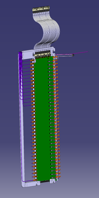
The HV and the anode signals of each column of the detector is routed through a PCB board. This boards also holds one LED per channel.
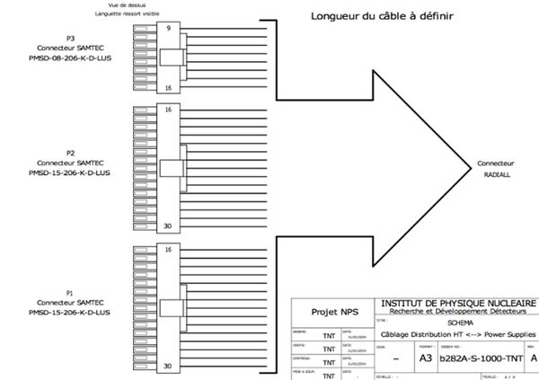
- The HV is distributed from the top of the board through 3 ribbon cables.
- The LED sitting in front of each PMT are controlled by a ribbon cable connecting at the bottom of the board
- Anode signal from each channel get out of the board through the opposite side and through SMA connectors
- Board schematics: 1, 2
HV ribbon cables
LED control cables
Anode signal cables
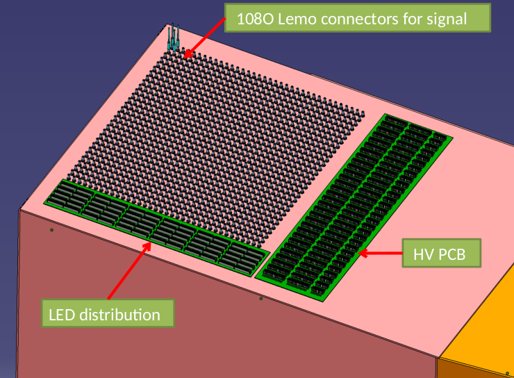
Patch panels at the top of the NPS box
There are 3 panels of the top of the NPS box:
